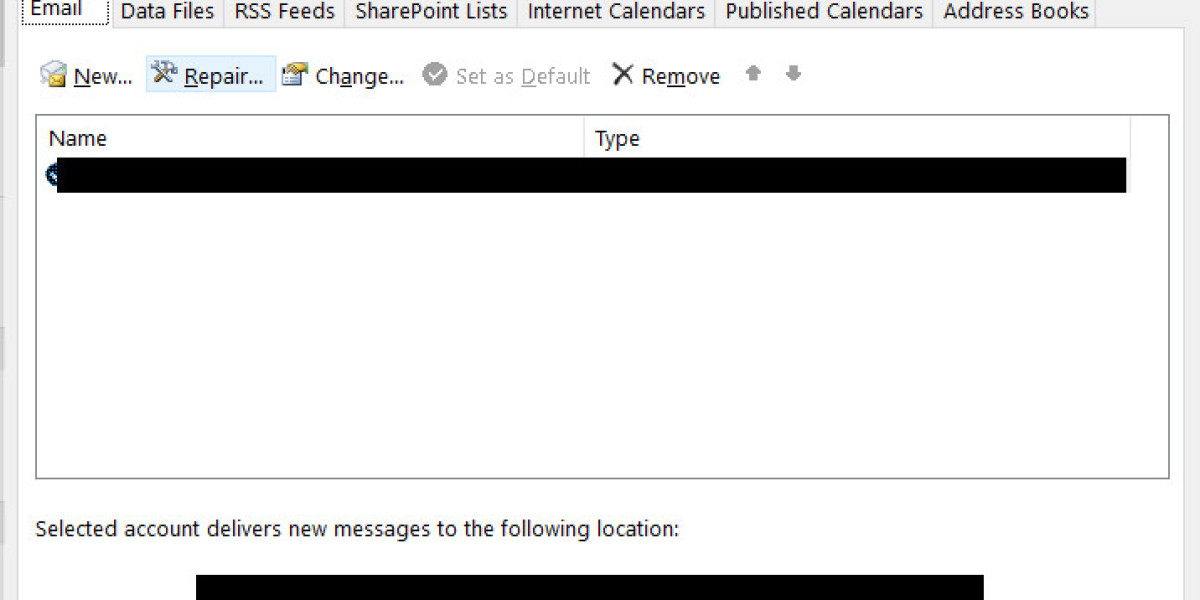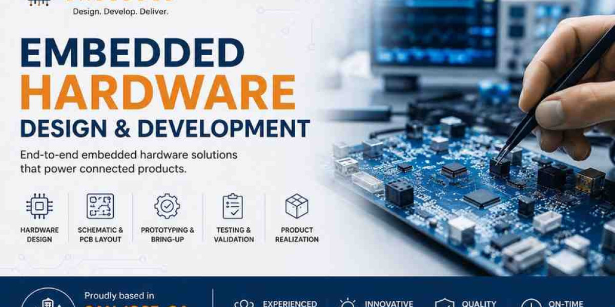
The rapid evolution of computing systems, edge artificial intelligence, and autonomous technology demands an uncompromised approach to electronic systems engineering. From high-density computing clusters in North San Jose and biomedical devices in Downtown San Jose to industrial automation grids across Silicon Valley, embedded hardware forms the literal physical engine of modern tech infrastructure. Tasked with processing massive data streams, running low-latency machine learning models, and operating continuously in harsh environmental conditions, modern electronics require precise layout physics and micro-architectural optimization.
At Jenex Technocrats, we bridge the gap between initial conceptual system design and high-volume commercial production. Operating as the premier embedded hardware design company in San Jose, CA, our expert engineering teams deliver multi-layer PCB layouts, high-speed system-on-chip (SoC) integrations, and ruggedized edge compute engines tailored exactly to your operational specs. By pairing advanced simulation modeling with strict design-for-manufacturability (DFM) rules, we build fault-tolerant electronic hardware that effortlessly satisfies international compliance standards and drives down your production lifecycle costs.
1. Electrical Material Science: Navigating High-Speed Signal Integrity Physics
The single greatest point of failure for modern multi-layered circuit boards is a lack of high-speed signal integrity engineering. As clock speeds surge past $1\text{ GHz}$ and rise times drop into the picosecond range, standard PCB traces stop acting like simple copper wires and begin behaving like active radio-frequency transmission lines. Without exact impedance matching, signal loops suffer from signal reflections, cross-talk, and extreme electromagnetic interference (EMI) that can cause system reboots, data loss, and failed regulatory tests.
Our engineering teams eliminate these performance liabilities at the schematic and layout level:
Controlled Impedance Modeling: We utilize advanced field solvers to calculate exact trace widths and spacing geometries based on dielectrics like FR-4 or Rogers materials, guaranteeing uniform impedance tracking across the board.
Complex Layer Stackup Optimization: We design robust multi-layer boards (ranging from 4 to 32+ layers) using dedicated ground and power planes to block cross-talk and isolate sensitive analog traces from noisy digital buses.
Advanced High-Speed Bus Routing: Our layout designers use length-matching, differential pair tracking, and via-stitching protocols to cleanly route high-speed buses like PCIe Gen 5, DDR5, and USB4.
Internal Structural Link: Discover our comprehensive software engineering capabilities that seamlessly drive this custom architecture by reading our guide to Embedded Firmware Development.
2. Full-Service Turnkey Embedded Hardware Competencies
Our high-production layout, prototyping, and optimization pipelines are engineered to handle the complete design lifecycle of your next-generation electronic assets.
I. Processing Architecture Engineering
The Integration: Configuring low-power microcontrollers (such as ARM Cortex-M), ultra-high performance application processors, or flexible FPGA matrices matched to your system's data-throughput requirements.
The Benefit: Eliminates component bottlenecking while optimizing thermal and energy consumption boundaries across the board.
II. Custom Wireless & RF Integrations
The Integration: Tuning integrated on-board antennas and RF circuitry for ultra-reliable communication links, including Wi-Fi 6E/7, Bluetooth Low Energy (BLE), cellular 5G, LoRaWAN, and satellite positioning.
The Benefit: Delivers continuous data transmission in dense, high-interference urban or industrial environments.
III. Power Management IC (PMIC) Optimization
The Integration: Engineering custom multi-rail power distribution networks using buck-boost regulators, low-dropout (LDO) regulators, and smart battery charging topologies.
The Benefit: Maximizes battery life for remote edge sensors and handheld devices while safely isolating volatile current spikes.
IV. Sensor Fusion & Analog Front-End (AFE) Design
The Integration: Designing precision analog-to-digital filtering arrays to sample data from complex arrays of LiDAR, cameras, medical monitors, or industrial telemetry.
The Benefit: Cleans and processes weak real-world signals into high-fidelity digital streams before they reach the main processing core.
Internal Structural Link: Learn how we scale these custom system designs into field-ready enterprise frameworks by checking out our Internet of Things (IoT) Solutions catalog.
3. Structural Matrix: Enterprise Engineering vs. Hobbyist Layouts
Partnering with an established, hardware design agency ensures your system scales seamlessly from prototype validation to high-volume contract manufacturing runs.
| Engineering Performance Vector | Low-Tier Hobbyist Layout Design | Jenex Enterprise Engineering Standards |
| Multi-Layer PCB Capacities | Limited to 2–4 standard layers | 4 to 32+ High-Density Layers (HDI) |
| High-Speed Bus Optimization | Auto-routed without trace math | Length-matched differential pairs |
| Thermal Dissipation Management | Basic heatsinks, high hotspots | Thermal vias, copper pours, 3D thermal modeling |
| Regulatory Pre-Compliance | Ignored (Prone to FCC test ruin) | In-house EMI/EMC virtual testing |
| Component Lifecycle Assurance | Uses obsolete or rare parts | Full supply-chain longevity audits |
4. Rigorous Compliance Engineering: FCC, CE, and ISO Standards
Bringing a commercial electronic product to market in Silicon Valley requires strict adherence to international certification laws. Emitting excessive radio interference or lacking electrostatic discharge (ESD) protection will cause your product to fail certification checks, leading to major redesigns, lost revenue, and project delays.
Our engineers execute strict compliance screening protocols throughout the layout cycle:
EMI/EMC Shielding Enclosures: We place custom metal shielding cans, guard traces, and filtering chokes around high-frequency circuits to block outgoing radio emissions and prevent incoming interference.
Transient Overvoltage Protection: We build arrays of TVS diodes, varistors, and gas discharge tubes directly into input/output ports to absorb static electricity shocks and power surges without blowing out expensive internal components.
Medical & Industrial Isolation: For specialized industrial and medical products, we design physical creepage and clearance air gaps into the circuit layout to satisfy strict high-voltage safety rules.
Internal Structural Link: See how we transition these hardened circuit patterns into optimized physical shapes by viewing our Custom Enclosure & Mechanical Design services.
Frequently Asked Questions (FAQ)
Q: What is the main benefit of partnering with an outsourced embedded hardware design company?
A: Developing complex hardware requires a specialized group of tools and engineers, including signal integrity experts, RF layout designers, power management specialists, and compliance engineers. Outsourcing to an enterprise design firm gives you immediate access to a complete team, advanced engineering tools, and established contract manufacturing networks, bypassing the high costs and setup times of building an in-house hardware division.
Q: How do your hardware crews manage component shortages and supply chain risks?
A: Component sourcing issues can stall an entire production line if a critical chip goes out of stock. We protect your project during the schematic phase by running thorough supply chain audits. We only pick parts that feature multi-year factory roadmaps, high inventory numbers, and pin-compatible backup choices from alternative manufacturers, ensuring your board can be built continuously.
Q: Can you help adapt our current electronic product for high-volume manufacturing?
A: Yes, absolutely. We specialize in updating older or prototype-level designs into high-yield, production-ready boards. Our team analyzes your circuit layout to reduce component count, shift parts to standard surface-mount (SMD) packages, remove expensive manual assembly steps, and optimize the overall trace layout for rapid automated pick-and-place assembly machines.
Conclusion: Secure Your Product’s Physical Infrastructure
Your hardware layout dictates your system's operational stability, energy efficiency, and long-term market profitability. Do not risk your venture capital funding or corporate reputation by trusting your electronic engineering to general programmers or uncertified layout artists who lack deep physical building science experience. Rely on the high-production capacity, modern commercial simulation equipment, and surgical accuracy of Silicon Valley’s premier electronics engineers.
? Ready to Secure Your Free Hardware Architecture Audit? Call us at +1 079-4940-7293 or visit Jenex Technocrats today to submit your product design goals, upload block diagrams, or lock in an expert technical consultation with our specialized team.
Follow us on or Our Social Media Links:
Stay updated with our latest high-speed PCB layouts, firmware optimization breakthroughs, and commercial hardware production updates across Silicon Valley:
Facebook: Jenex Technocrats
Instagram: @jenextechs
X (Twitter): @jenextech
LinkedIn: Jenex Technocrats